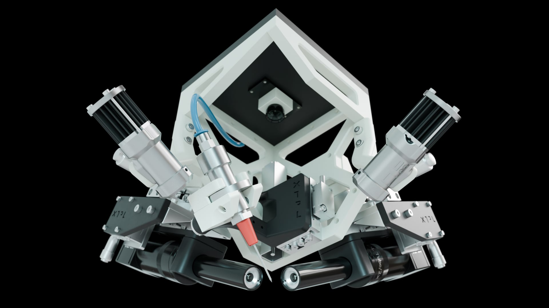
Quick Summary
Additional Context
Chip packaging refers to all parts of a semiconductor device aside from the die (the “chip”) itself. As this IBM explainer nicely puts it, “In a nutshell, chip packaging provides the mechanical environment where a computer chip operates.” Advanced packaging refers to solutions where the components that house a chip aren’t only providing a protective environment, but are also part of the chip’s functionality.
The breakthroughs in advanced packaging have largely resulted from the 3D design revolution in semiconductors over the last couple of decades, which has led semiconductor device manufacturers to increasingly explore the potential advantages of stacking chips vertically instead of exclusively side-by-side. This background accounts for why it’s more and more common for additive manufact